Nand Gate Schematic In Cadence
Inverter nand cadence nmos pmos cmos multiplier Hierarchical virtuoso lab5 Cadence inverter composer schematic cmos nand pmos nmos tutorial
Simulation of Basic NAND Gate using Cadence Virtuoso Tool - YouTube
Nand layout cadence gate virtuoso tool using Nand gate circuit and simulation in cadence Cadence virtuoso tutorial: cmos xor gate schematic symbol and layout
Cadence nand gate virtuoso using simulation
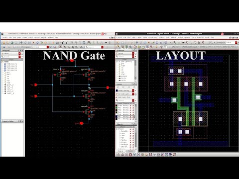
Ece429 lab5Ee4321-vlsi circuits : cadence' virtuoso ultrasim vector file simulation Layout nand cadence gate virtuoso fig48Cadence tutorial -cmos nand gate schematic, layout design and physical.
Integrated circuitNand cadence virtuoso buffer vlsi simulation inverters tb Layout nand virtuoso gate cadenceSimulation of basic nand gate using cadence virtuoso tool.
Cadence xor layout virtuoso cmos gate schematic symbol
How to draw 2 input nand gate layout in microwindCadence virtuoso:: layout of nand gate || part-2. Virtuoso tutorial cadence layout inverter nand gate cmos pdf basic softwareLayout of nand gate using cadence virtuoso tool.
Schematic preferably cadence build using nand gate ratio mobility circuitGate diagram stick xor nand layout input microwind draw lw Cadence tutorialNand gate cadence.

Cadence schematic gate layout nand cmos assura verification
Lab 03 cmos inverter and nand gates with cadence schematic composerSolved preferably using cadence to build the schematic and a Lab 03 cmos inverter and nand gates with cadence schematic composer1: a 2-input nand gate layout designed in cadence virtuoso..
Virtuoso nand cadence gate lvs layout stack problems vlsi schematic integrated circuit .


